Why is tantalum an ideal material for semiconductor chips?
Tantalum has very stable thermal, electrical and mechanical properties and can be used in a wide temperature range for semiconductor processing. Its compatibility with silicon and silicon dioxide is a big plus.
Tantalum primarily acts as a diffusion barrier between the copper seed layer and silicon, producing the unique adhesion properties of silicon and copper without chemically reacting with the copper matrix. The diffusion barrier is usually a multilayer structure of pure tantalum, tantalum nitride.
The versatility of tantalum allows it to be used in large numbers in diffusion barrier applications for copper interconnects. While other materials could in principle be used for the same purpose, rapid advances in semiconductor technology and "Moore's Law" (an observation that the number of transistors in dense integrated circuits doubles roughly every two years) have made tantalum a highly stable, Preferred material with few machining problems.

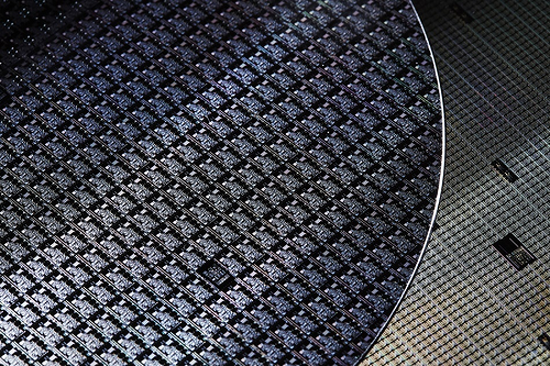
The surface of the semicircular wafer. The unique properties of tantalum make it an important part of advanced electronics.
What are the different roles played by tantalum in semiconductor technology?
How is tantalum introduced into semiconductor surfaces?
The tantalum ion implantation layer was prepared by a new tantalum ion implantation process extended by the CVD vapor deposition and CVI vapor infiltration technology of Ains (Beijing) Tantalum Application Technology Co., Ltd.

silicon wafer. Tantalum ions are implanted into silicon, allowing a copper layer to be placed on top without diffusion between the metal (copper) and semiconductor (silicon) layers.
The main function of the diffusion barrier is to prevent contamination of the underlying silicon from the conductor material (copper or aluminum).
Typically, titanium and aluminum are used together, and tantalum and copper are used together. When titanium reacts with copper, intermetallic compounds form poorly, while tantalum and copper are completely incompatible.
Tantalum and titanium also have good adhesion properties to silicon, improving the adhesion of copper or aluminum to the substrate. Both tantalum and titanium can be deposited in pure metal or nitride conditions, or can be fine-tuned in conjunction with the interface between silicon and copper or aluminum to control the properties of the deposited seed material.
In large-capacity capacitors with very high specific surface area, sintered tantalum powder forms a conductive mass, and the surface is anodized to form a stable insulating tantalum oxide layer.
In this way, very high capacitance per unit volume can be obtained with very short conduction paths. Since the electrical properties of tantalum are very stable with temperature, the capacitance does not change much in the actual use range.
This feature becomes especially important in demanding outdoor applications, such as the automotive and telecommunications industries. The short conduction paths allow very fast loading and unloading, allowing buffering of input and output signals from the integrated circuit at all frequencies.

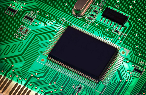
capacitors on the motherboard. Tantalum capacitors have high capacitance and short conduction paths per unit volume.
The use of tantalum in other exciting applications!
The incompatibility and high ductility of tantalum with copper serve as a diffusion barrier for A15 superconductor materials, and as reinforcement and reinforcement elements in superconductor wires and cables.
Tantalum can be alloyed with tungsten to make it stronger, yet remain highly ductile, and has a variety of uses in high-performance chemical and aerospace applications.
The chemical inertness of tantalum, especially near room temperature, makes tantalum compatible with the human body, which means it can be used in medical implants. Tantalum also has unique mechanical properties that can be used in defense applications.
Tantalum can be supplied as an alloy, as a solid or as a porous structure.
Tantalum can be deep drawn into a variety of shapes for many applications. Tantalum powder can be used in a variety of additive manufacturing processes.